This is a writeup of my spare time experimenting with a voltage and current calibrator Model 8200 from manufacturer Data Precision (Analogic), which i found a few years ago at ebay. It provides (or: should provide) precise DC voltages programmable to 6½ digits, quite useful in the lab.
Beware, this text might contain serious flaws end errors. No warranty whatsoever! Mingle with the calibrator on your own risk.
This document is written in LaTeX, with drawings by Xfig, and processing through make4ht. There is also a PDF version (A4 paper) of this document for download.
The calibrator service manual as PDF file can be found, e. g., at KO4BB. When the calibrator arrived, it worked fine at the first glance, but upon closer look it had at least a noise issue. First i suspected the culprit to be the relay contacts, but after cleaning them the noise problem remained. It took me a while to find out that a Mica capacitor, C17 in the Schematic A1, produced some burst or telegraph noise. After its replacement by a new capacitor of the same type (still available!), i tried to adjust the box after the procedure given in the Instruction Manual 62-5018. Happily i could use a 8½-digit DMM FLUKE 8588A, thanks to our company vH&S, and adjustment worked fine. Only at the final step, the carry adjustment, one potentiometer was at its end stop already and still no correct carry adjustment could be reached, with a few hundred microvolts error. That means, that in effect one can forget the entire adjustment, and the calibrator is useless due to its lacking accuracy. Obviously something had aged during the 30 years since production, beyond what can be adjusted by the potentiometers.
Then there were two possibilities: Either mingle with the resistors until it somehow fits, or first find out about the underlying DAC principle, and how the many reference voltages and resistors relate to each other. Eventually then it should be possible to understand, which resistor to replace and which resistance it must have. This is described in Sec. 2 below.
While playing with the calibrator, i found that there are a few very nice videos on youtube regaring another, successful repair. Keith Noneya shows in quite some detail how to disassemble, clean, and reassemble the digit switches. His instructive videos can be found through these links:
Many thanks to Keith for his fresh rendering, correction, and annotation of the calibrator schematics.
The current status of my Model 8200 here is, that the calibrator is still not fixed, since one precision-critical resistor likely needs to be procured. This is not dramatic, since the calibrator itself is such an ingeniously designed piece of classic hardware, and there are quite a few things to learn from it. So this is a slowly ongoing story, glacially slow, that is.
The following text is concerned with the DAC part of the calibrator, its fixing and adjustment.
As shown in Schematic No. 65-1029 (A1), the analog DAC output is calculated from a digital input of seven octal digits. These are calculated by the included microcontroller from the decimal digits as they are set at the front panel or through the IEEE interface. Each such octal digit of 3 bit has a numeric range of 0…7, and so the DAC has a resolution of 7 ⋅ 3bit = 21bit. But since for one polarity only 20 bits can be set by the user, the Schematic A1 calls it a 20 bit DAC.
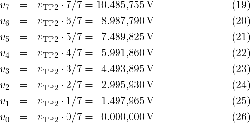
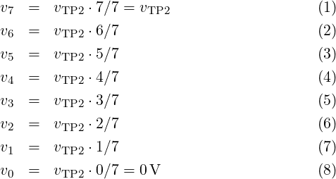
For D/A conversion, this DAC type needs eight reference voltages, increasing by equal steps, which are generated from a main reference voltage by a resistive divider chain. Since this main reference voltage in the Schematic appears at test point TP2, it is named vTP2 here, and the eight reference voltages are:
These voltages are adjusted by 20-turn potentiometers R18, R21, R24, R27, R30, and R33. The tiny Lua program dac-trimpot.lua calculates the nominal position of these potentiometers, that is, if all resistors would have their ideal value. The program output is as follows:
It shows, that all pots but R18 are nominally at their mid position, and that these have an adjustment range of approx. ±250μV. The program output also shows, that resistor R18 is nominally rather near to its end stop.
The reference voltages v0…v7 are the inputs for seven octal analog-multiplexer ICs (Z7…Z13). Depending on the octal digit at each multiplexer, one of the voltages v0…v7 is routed through to the multiplexer output, where it is buffered by an operational amplifier (Z14…Z18). With each of the 21 DAC input bits A0…A20 having either value 1 (logic high) or value 0 (logic low), the seven multiplexer output voltages are calculated as follows:
The buffered multiplexer output voltages are fed into a resistor network, shown in Fig. 1. Its purpose is to combine the seven voltages, while weighting them by factors 8k, with integer k, and by this generating the DAC output voltage vDAC. This network has a few added resistors and potentiometers for adjustment of proper 8k relations. Actually it’s a combination of a DAC for the lower 12 bits (vZ10…vZ13) with a DAC for the higher 9 bits (vZ7…vZ9), combined by resistor R44.

The circuit architecture in Fig. 1 avoids increasingly high resistors for the lower DAC bits, which are needed there since the lowest multiplexer voltages, e. g., vZ13, must have only very small influence on vDAC. If one would build such a 21 bit DAC only with resistors staggered by factors 8k, a network with identical function to the one from Fig. 1 would look like the one in Fig. 2. Then with, e. g., R = 1kΩ for vZ7, the resistor for vZ13 would have the value 86 ⋅ R = 262.144MΩ.

Such large resistor values as needed in in Fig. 2 are very difficult to manufacture with high accuracy and low thermal coefficient, whereas in Fig. 1 the resistors remain low, below 1MΩ, and the most accuracy-critical resistors for vZ7, vZ8 and vZ9 can be built from bulk metal foil, with almost zero temperature coefficient and very low drift.
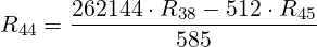
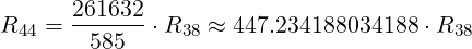
In Fig. 1 the lower and higher DAC part are connected by resistor R44. The question is, which value R44 must have? From R38 = 1kΩ one knows that the combined resistance (R39 + R40)||R41 = 8 ⋅ R38 = 8kΩ, and R43 + R44 = 82 ⋅ R38 = 64kΩ. So for the upper DAC part all depends on R38. Similarly for the lower DAC part, R46 = 8 ⋅ R45, R47 = 82 ⋅ R45, and R48 = 83 ⋅ R45. With R45 = 1kΩ, R46 = 8kΩ, R47 = 64kΩ, and R48 = 512kΩ result.
With all resistors depending on either R38 or R45, the value R44 will be a function of both R38 and R45. It is not needed that R38 = R45 as it’s done in the calibrator; instead one could dimension the lower DAC part differently from the upper one. Then only R44 would need to be adapted.

For calculation of R44, it is assumed for a moment, in Fig. 3, that vDAC is somehow held at 0 V (virtual GND), further vZ8 = vZ9 = vZ11 = vZ12 = vZ13 = 0V. For the case where vZ7 = 1V and vZ10 = 0V, the ground current iGND must be 83 = 512 times the ground current for the case where vZ10 = 1V and vZ7 = 0V. The following tiny maxima program provides the value of R44:
| (16) |
With R46 = 8 ⋅ R45, R47 = 82 ⋅ R45, and R48 = 83 ⋅ R45, this simplifies to:
| (17) |
With R45 = R38 it simplifies further:
| (18) |
This corresponds well with the value of R44 in the Service Manual.
Now the reference voltage vTP2 is calculated. The Schematic No. 65-1029 shows, that DAC bit A0 is special: For positive calibrator output voltage it is always logic low, and for negative calibrator output voltage it is always logic high. For DAC programming then only 20 bits remain, which is the reason why the Schematic tells that it’s a 20 bit DAC.
The 20 bit word B0…B19 at the DAC input provides ‘programming’ LSB steps of 10μV for the user, whereas the real ‘DAC’ LSB size of the 21 bit DAC is 5μV. The correspondence between the DAC bits A0…A20 and the programming bits B0…B19 is shown in Table 1.
| DAC | Prog. | MUX | MUX | |
| Bit | Bit | IC | Pin | |
| A20 | B19 | Z7 | 9 | MSB |
| A19 | B18 | Z7 | 10 | |
| A18 | B17 | Z7 | 11 | |
| A17 | B16 | Z8 | 9 | |
| A16 | B15 | Z8 | 10 | |
| A15 | B14 | Z8 | 11 | |
| A14 | B13 | Z9 | 9 | |
| A13 | B12 | Z9 | 10 | |
| A12 | B11 | Z9 | 11 | |
| A11 | B10 | Z10 | 9 | |
| A10 | B9 | Z10 | 10 | |
| A9 | B8 | Z10 | 11 | |
| A8 | B7 | Z11 | 9 | |
| A7 | B6 | Z11 | 10 | |
| A6 | B5 | Z11 | 11 | |
| A5 | B4 | Z12 | 9 | |
| A4 | B3 | Z12 | 10 | |
| A3 | B2 | Z12 | 11 | |
| A2 | B1 | Z13 | 9 | |
| A1 | B0 | Z13 | 10 | |
| A0 | Sign | Z13 | 11 | LSB |
A few examples of octal DAC input values nDAC,oct, their decimal values nDAC,dec, and the resulting DAC output voltage vDAC are shown in Table 2. The ones marked with ∗ are the actually programmable ones, multiples of 10μV.
| nDAC,oct | nDAC,dec | vTP3 | Set |
| 0000000 | 0 | 0.000,000 V | ∗ |
| 0000001 | 1 | 0.000,005 V | |
| 0000002 | 2 | 0.000,010 V | ∗ |
| 0000003 | 3 | 0.000,015 V | |
| 0000004 | 4 | 0.000,020 V | ∗ |
| 0000006 | 6 | 0.000,030 V | ∗ |
| 0000010 | 8 | 0.000,040 V | ∗ |
| 0000012 | 10 | 0.000,050 V | ∗ |
 |
 |
 |
|
| 7777766 | 2097142 | 10.485,710 V | ∗ |
| 7777770 | 2097144 | 10.485,720 V | ∗ |
| 7777772 | 2097146 | 10.485,730 V | ∗ |
| 7777774 | 2097148 | 10.485,740 V | ∗ |
| 7777775 | 2097149 | 10.485,745 V | |
| 7777776 | 2097150 | 10.485,750 V | ∗ |
| 7777777 | 2097151 | 10.485,755 V |
As one can see, with 221 = 87,

and so all reference voltages are defined:
All these voltages are multiples of 5μV, since 221 − 1 is divisible by seven: (221 − 1)∕7 = 299593.
Another way to calculate vTP2 is, to use the network Fig. 2 and let it output the smallest non-zero voltage, vDAC = 5μV. This requires vZ13 = vTP2∕7, and all other vZ12 = vZ11 = vZ10 = vZ9 = vZ8 = vZ7 = 0V. Then the network is supplied only through resistor 86 ⋅R, while all other resistors in parallel are connected to ground. This voltage divider can be calculated easily, e. g., by a tiny maxima program as shown in the following listing.
Running this program gives:
When the calibrator is programmed to output a negative voltage, the DAC still produces a non-negative voltage, but the entire DAC part, including reference voltage regulator, is anchored differently relatively to the LO side calibrator terminal. The polarity switching is illustrated in Fig. 4.

The shown double-throw switch is actually a pair of MOSFETs, Q9 and Q10 in Schematic A1. In the switch position shown (Q9 conducting), The v7 point (TP2) is connected to Pwr RET, which is also the LO terminal. When the DAC is commanded to its full-scale value, that is, 7777777oct, all multiplexers route the same voltage v7 through to the DAC network, so that in effect the voltage at point TP3 is 0 V. When the DAC is commanded to one step less, 7777776oct, the point TP3 shows −5μV. With an DAC programming value of 7777775oct, the point TP3 is at −10μV. A programming value of 7777773oct results in −20μV at TP3. So any positive DAC output voltage other than the fullscale value appears at TP3 as a negative voltage relative to Pwr RET. It is then buffered by op-amp Z19 similarly to a positive voltage, since Z19 has a bipolar power supply.
For negative calibrator output voltages, all multiples of −10μV have the DAC bit A0 set to logical high; for positive calibrator output the bit A0 is always logical low. In the circuitry this is simply reached by connecting A0 to Pwr RET, so its voltage relative to the floating GND of the DAC is either 0 V or v7, which counts as logic high for the CMOS multiplexers.
| nDAC,oct | nDAC,dec | vTP3 | Set |
| 7777777 | 2097151 | −0.000,000 V | ∗ |
| 7777776 | 2097150 | −0.000,005 V | |
| 7777775 | 2097149 | −0.000,010 V | ∗ |
| 7777774 | 2097148 | −0.000,015 V | |
| 7777773 | 2097147 | −0.000,020 V | ∗ |
| 7777771 | 2097145 | −0.000,030 V | ∗ |
| 7777767 | 2097143 | −0.000,040 V | ∗ |
| 7777765 | 2097141 | −0.000,050 V | ∗ |
 |
 |
 |
|
| 0000011 | 9 | −10.485,710 V | ∗ |
| 0000007 | 7 | −10.485,720 V | ∗ |
| 0000005 | 5 | −10.485,730 V | ∗ |
| 0000003 | 3 | −10.485,740 V | ∗ |
| 0000002 | 2 | −10.485,745 V | |
| 0000001 | 1 | −10.485,750 V | ∗ |
| 0000000 | 0 | −10.485,755 V |
Comparison of Table 2 and Table 3 shows that programming a negative voltage vTP3 requires, that MOSFET Q9 is conducting instead of Q10, and that the DAC is programmed with the ones’ complement of the value for the same, but positive voltage. Just each programming bit needs to be inverted. So in positive and negative calibrator output mode, the 5μV steps of the 21 bit DAC would be available, as the DAC provides them, but they are not programmable.
When the Model 8200 calibrator was designed, obviously around 1980 as seen in the Schematic sheet, there were already other DACs available. The majority of these were typically based on R2R resistor ladder networks, where only resistors of two distinct values, R and 2R, would be needed. But what made the designers of this Model 8200 calibrator choose an octal-digit DAC principle instead?
Here are a few guesses: It’s a matter of optimization with the material available at the time. The CMOS 4000 logic series was already widely available and cheap, and beyond mere logic functions it included also several cool mixed-signal and analog (!) functions, like a PLL (CD4049), and particularly MOS switches (e. g., CD4016) and multiplexers (e. g., CD4051). The latter are essentially offset-free, a very nice feature, and they provide a direct resistive signal path from input to output. So it was cheap to route one out of eight available reference voltages v0…v7 to some place in the DAC circuit by CMOS analog multiplexers.
The op-amps at that time were likely much more expensive, and they were at their performance limits regarding linearity, offset voltage, and offset drift. So one would try to build the DAC with the minimal amount of expensive precision op-amps.
If one would use an R2R network, each of the highest DAC bits would need such a precice op-amp as buffer after the reference voltage switch. Now looking to the architecture of the Model 8200, there is only one precision op-amp (Z14) for the highest three DAC bits needed. Three bits lower the precision requirements are already more lenient, only 1∕8 regarding offset and linearity for the buffer op-amp (Z15) there. So the octal-digit DAC principle spares expensive op-amps. Similarly, instead of two precision resistors per bit for an R2R network, the octal-digit DAC needs only one precision resistor per three bits. In addition the DAC needs once a set of seven non-zero reference voltages v1…v7, which amounts to seven identical precision resistors. In total, the octal-digit DAC needs a smaller amount of precision resistors than a comparable R2R DAC.
Another aspect is, how complex the DAC calibration would be. Calibrating the eight reference voltages is straight-forward, as the voltages are generally large and well measurable, or comparable to the voltages derived by a standard resistor divider network. Eight potentiometers are needed for this adjustment. The remaining DAC network behind the multiplexers contains only eight resistors with decreasing precision, which is well feasible. Where resistor tolerances are too large for the required accuracy, a few potentiometers are needed. But obviously with only two potentiometers (R39 and R42), it should be possible to adjust the entire DAC.
So it seems designing an octal-digit DAC was a well-thought choice, an optimization likely based not only on technical, but also on financial calculations. It’s elegant.
For calibrator adjustment, accurately measuring the voltage at test point TP3 is essential. But there is only a solder pad TP3 on the PCB. To have a robust, pluggable connection to TP3, i soldered a gold-plated 2 mm connector (type SA200, order-no. 22.1100, from manufacturer Stäubli) vertically to the solder pad, after having cut and ground away its M2 thread part.
There are two points, where the offset voltage of the calibrator needs to be zeroed. The calibrator offset voltage is independent from the DAC setting.
In a first step, by potentiometer R37 at op-amp Z14 not only the offset voltage of Z14 is trimmed away, but also the offsets of all other op-amps Z15…Z18. Obviously the offset of Z15 influences the output offset only by  of the one from Z14, the influence of Z16 is only
  of
the one from Z14, and so on for the four op-amps within Z17 and Z18. This allows to use op-amps with increasingly larger offset voltages than Z14 for the lower digits. As a result, when the calibrator is programmed to 0 V, the test point TP3 must show 0V ± a few μV.
of
the one from Z14, and so on for the four op-amps within Z17 and Z18. This allows to use op-amps with increasingly larger offset voltages than Z14 for the lower digits. As a result, when the calibrator is programmed to 0 V, the test point TP3 must show 0V ± a few μV.
Between TP3 and the calibrator output there is op-amp Z19, which is the remaining source for offset voltage. After R37 is adjusted of zero offset at TP3, in a second step the same needs to be done for R60 at Z19 until the calibrator output shows approx. 0μV. The op-amp Z20 does not influence the output offset voltage, since it’s inside the control loop by Z19. Also the 100 V amplifier is inside the same control loop, so it does not need a separate offset trimming either.
The Service Manual in Sec. 4.3 describes the calibration procedure. It requires a precision divider network (JRL DMR105, or equivalent), whose purpose is, to divide the voltage of a voltage standard into 8 exactly equally spaced voltages. Then the calibrator needs to be set to one of these eight voltages, and by a null voltmeter (with microvolt resolution) the calibrator output is compared against the voltage at the corresponding divider tap.
With divider tap the contacts at the external precision divider network are meant — but not any measurement point inside the calibrator.
For each voltage a dedicated potentiometer in the calibrator needs to be adjusted (see Table 4-1 in the Service Manual) until the null voltmeter shows zero Volt. Then the calibrator output voltage for the given voltage setting is identical to the voltage at the corresponding tap of the precision divider network.
This procedure requires three special tools, a divider network, a voltage standard, and a null voltmeter. Nowadays one can simply measure the calibrator output by a 7.5 digit (or better) DVM and check that the calibrator voltage fits to the corresponding setting value from Table 4-1 in the Service Manual.
But why are the voltages from Table 4-1 chosen for linearity adjustment? Converting these voltages into the corresponding DAC input values nDAC,oct values gives a clue. Here is the bit pattern at the multiplexers, calculated with a Lua function, part of the library described in Sec. 4 :
As one can see, for each of the linearity adjustment voltages the multiplexers Z7…Z12 route the same reference voltage (one out of v0…v7) to the network, while multiplexer Z13 — the one with the least effect — outputs 0 V. E. g., for 1.49796 V, multiplexers Z7…Z12 output v1. By using these particular voltage values, all resistors but the least significant one are effectively connected in parallel, so that the DAC network is almost without divider function.
There is only a minute influence by the resistor coming from Z13, which pulls the result slightly towards zero. Its influence can be easily seen by extending the table until full-scale is reached:
The Schematic No. 65-1029 (A1) does not tell a sequence for adjustment of the potentiometers. If done in a non-optimal way, adjustment of some potentiometer may need to re-adjust others. The voltage v1 is influenced only by potentiometer R12, but as a global scaling this influences all other adjustments. Therefore it must be done first. By this adjustment also the voltage at the upper wire of R26, the inverting input to op-amp Z6, is fixed. When v1 has been adjusted through R12, potentiometers R27, R30, and R33 can be adjusted independently from each other and from other later adjustments. Adjusting potentiometer R18 wired as a variable resistor (not as a voltage divider) influences the settings of R21 and R24 (but not R27, R30, and R33) so it should be adjusted before R21 and R24.
The following seems to be one sequence, where no potentiometer adjustment is influenced by a later one.
| Adjusts | DAC | ||
| Step | Potentiometer | Ref.-V. | Setting |
| 1 | R12 | v1 | 1.49796 V |
| 2 | R18 | v7 | 10.48572 V |
| 3 | R27 | v4 | 5.99184 V |
| 4 | R30 | v3 | 4.49388 V |
| 5 | R33 | v2 | 2.99592 V |
| 6 | R21 | v6 | 8.98776 V |
| 7 | R24 | v5 | 7.48980 V |
For adjustment, the calibrator needs to be set to the listed voltages, and the corresponding potentiometer needs to be trimmed until the voltage appears a the calibrator output. After one has successfully done the linearization adjustment, the reference voltages v0…v7 will have the values calculated in Eqn. 19 …Eqn. 26.
Critical points in the DAC conversion curves appear at adjacent octal programming values or voltage steps, where a higher-significant multiplexer takes over, while all lower-significant multiplexers flip to zero output. Also at these voltages the step size of 10μV needs to be maintained. This potential cause for nonlinearity is linked to the particular DAC type, here the one based on octal analog multiplexers.
The Fig. 1 shows two potentiometers, R39 and R42, which allow to fix the 10μV step size at two most critical transitions. The following table shows, which multiplexer settings correspond to the special voltages mentioned in Sec. 4.3.5 Carry Adjustment of the Service Manual:
Obviously there are more voltages, where potentially critical carry errors can occur, e. g., the transition between 0.02047V and 0.02048V, but there is no potentiometer for adjustment.
Once the calibrator is fully adjusted, its overall performance, particularly linearity can be measured. This is done here with the help of a small Lua program dac-nonlin.lua in combination with a Lua library described below in Sec. 4. The process is as follows:
In a first step, measure the calibrator output voltage in the 10 V range for all voltage settings, where only the most significant multiplexer Z7 provides a voltage to the DAC network, while the other six multiplexers output 0 V. These particular calibrator voltage settings, which must appear on its display, are:
| 0.00000 V |
| 1.31072 V |
| 2.62144 V |
| 3.93216 V |
| 5.24288 V |
| 6.55360 V |
| 7.86432 V |
| 9.17504 V |
The calibrator output voltage for each of these eight set voltages is measured and put into the Lua table v_highest_digit within program dac-nonlin.lua.
In the second step (well, steps can be interchanged), measure the calibrator output voltage for the maximum voltage that each of the multiplexer outputs Z7…Z13 can provide. Multiplexer Z13 is special, since here the maximum programmable voltage contribution is 30μV instead of 35μV, since the DAC input bit A0 is always logical zero for positive calibrator output. This special case is taken care of by the program dac-nonlin.lua. The particular calibrator set voltages for the second step are:
| 0.00003 V |
| 0.00028 V |
| 0.00224 V |
| 0.01792 V |
| 0.14336 V |
| 1.14688 V |
| 9.17504 V |
Also here, the actual calibrator output voltages for these seven set voltages are measured, and then put into the Lua table v_digit_max. The two sets of measured voltages, fifteen in total, are sufficient to analyze the nonlinearity of the calibrator, since the voltage influence from the lower-order multiplexers follows the nonlinearity of the v_highest_digit voltages, and the weights of all octal digits, as they are provided by the DAC network, are represented by the table v_digit_max.
Once these values are put into the Lua program, one has a simplified model of the calibrator DAC, which one can set to any voltage between 0 V and 10.485755 V and check its simulated output voltage. In the program this is generated for each set value by a for-loop over all seven octal (not decimal!) digits. Subtracting the ideal calibrator output voltage from the calculated one over the full DAC programming range provides a nonlinearity plot like the one shown in Fig. 5.

As can be seen, my Model 8200 calibrator in its current repair status provides output voltages within an error band of ±150μV, which is way too large. One should rather expect that with proper adjustment the calibrator error remains within a band of maybe ±10μV. So there is still work to do…
To simplify the analysis of the Model 8200 DAC, i wrote a small Lua library, libdac8200.lua. It provides a few utility functions listed below:
This function calculates the unloaded output voltage of the DAC resistor network in Fig. 1, when all seven voltages vZ7…vZ13 as well as all resistor values of the network are given. The function was generated by the small maxima program calc-v_tp3.mac.
This function calculates the resistor value R44 after Eqn. 16.
This function calculates the (bipolar) calibrator output voltage vout from given digital DAC input value nDAC (5μV increments) and calibrator output polarity.
This function calculates the DAC input value nDAC from given digital DAC programming value nprog (10μV increments) and calibrator output polarity.
This function calculates the (bipolar) output voltage vout of an ideal calibrator from given digital DAC programming value nprog (10μV increments) and calibrator output polarity.
This function calculates the DAC programming value nprog required to produce the given output voltage, which will be rounded into the raster of DAC output voltages.
This function calculates the input select digits of the seven multiplexers Z7…Z13 from given digital DAC input value nDAC (5μV increments).
This function uses function ndac2octal, but outputs the combined bit pattern of multiplexer select bits as a string.
This function outputs the eight reference voltages v0…v7 as they are listed in Eqn 19…26, for an ideal, error-free DAC.
This function simply prints all eight reference voltages v0…v7.
This function prints the pattern of multiplexer select bits for a few DAC programming values at the begin and end of DAC range, for the given calibrator output polarity.
This function prints the DAC programming values needed for linearization and carry adjustment.
This function prints a list with the DAC nonlinearity error for its full DAC range, after tables v_highest_digit and v_digit_max in program dac-nonlin-lua have been filled with the measurement results, as described in Sec. 3.5.
This function calls a few from the above functions for testing: Just remove the comment sign -- in front of the test() function call at the end of the library, and type lua lib8200.lua on the command line.
Since the Model 8200 was designed, electronics has steadily evolved. So it should be possible to improve the calibrator precision, making the calibrator more stable over time and temperature, or reducing the output noise. In the ideal case, a replacement of only a few components by modern ones would bring an improvement.
The calibrator schematics show that the components of the DAC and analog part have been selected to fit harmoniously together in their performance level. If one would want to improve the stability of the DAC, many components would need to be replaced. Particularly several custom-made or selected precision resistors would need an upgrade by significantly more expensive ones. Also the oven compensated reference voltage source Z5 (LM299) would need an upgrade.
Interestingly in 2021 an improved replacement for the venerable LM299 has appeared: the oven-compensated, buried Zener, 7.05 V voltage reference, type ADR1399. The table below shows a comparison by typical values, taken from the datasheets.
| Parameter | LM299 | ADR1399 |
| Nominal reference voltage | 6.95 V | 7.05 V |
| Reverse dynamic impedance | 0.5Ω | 0.08Ω |
| Temperature coefficient | 0.3ppm∕∘C | 0.2ppm∕∘C |
| Long term stability | 20ppm∕ |
7ppm∕ |
| Reference noise, peak-peak, | ||
| 0.1 Hz…10 Hz | 10μV | 1.44μV |
The table shows, that one can expect a significantly reduced low-frequent calibrator output noise, and the long-term voltage stability should improve as well. Both voltage references come with a similar, thermally shielded package, they are sharing the same pinout, and their heater circuits look almost identical, so the ADR1399 can be used almost as an drop-in replacement for the LM299. However a few points need to be considered as described below, if one wants to upgrade the voltage reference Z5 in the calibrator.
The nominal reference voltage of the ADR1399 is 100 mV higher than the LM299 one. By this difference an adjustment of the reference voltage v1 by potentiometer R12 might not be possible anymore. Then a change of selected resistors R9 and/or R10 will be needed.
The ADR1399 datasheet recommends an external compensation network built from a 5Ω resistor in series with a 1μF capacitor in parallel to the Zener circuit. Its soldering near Z5 should give no problem.
The LM299 Zener diode in the calibrator is supplied by a current of approx. 1 mA, whereas the ADR1399 datasheet recommends a Zener supply current of approx. 3 mA. This can be reached by reducing the value of resistor R7. With no other change, this additional current would be provided by op-amp Z6. Its then increased output current would give an increased heat dissipation, which might be disadvantageous for stability. Calculating the currents at the current node TP2 shows, that op-amp Z6 provides a current of 1.175 mA to the Zener reference through R7 plus a current of 3.001 mA into the reference divider chain. But also a positive current of approx. 3.7 mA flows from the +15V supply line through resistors R14 and R16 into node TP2, reducing the op-amp output current to positive 475μA.
So if one replaces the LM299 reference by an ADR1399, R9 and/or R10 might need replacement, R7 should be reduced to provide 3 mA Zener current, and both R14 and R16 should be reduced while keeping the quotient R14∕R16 about constant, so that op-amp Z6 will provide an almost unchanged output current of approx. 475μA.
Given the significantly reduced dynamic impedance of the ADR1399 Zener reference, one can also supply the active Zener directly from the +15V line through a differently wired resistor R7 of 2.67kΩ, as shown in the ADR1399 datasheet. The then reduced load for op-amp Z6 can be compensated by a 10kΩ resistor between test points TP2 and TP1, so that its output current will stay positive, around 475μA.
A few points to check when acquiring a used Model 8200 calibrator:
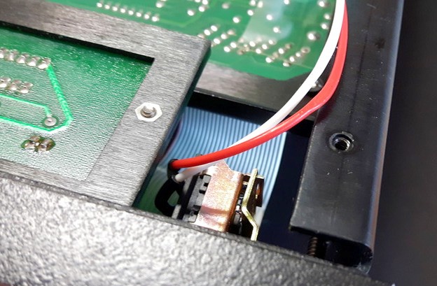
I found that, in my particular calibrator, the AC power wires were accidentally squeezed between the bottom cover plate and the side panel of the calibrator, see Fig. 6. The wire isolation looked still sufficient, but for more safety i put these AC wires into a spiral plastic cable wrap, where they go along the calibrator walls.
After any soldering it’s recommended (i do so) to clean the PCB, at least locally, using a stiff brush, 70 % isopropyl alcohol, and a blowgun, to remove resiny and salty residues. These might else give some high-ohmic creeping path, spoiling the accuracy. Before reassembly the PCB should be put into an oven at approx. 80∘C for a few hours, to remove moisture from the PCB material.
The following differences were spotted between the schematics and the actual calibrator hardware:
Nothing speaks against redesigning a DAC or even complete calibrator after the principle of the Model 8200 with more modern components. But it should be mentioned, that nowadays the entire DAC part of the calibrator fits into one IC. E. g., the DAC AD5791 from Analog Devices would be such a component. It has comparable accuracy, but it’s resolution is a bit lower, since its 20 bits span the full bipolar voltage output range, whereas the 21 bit DAC in the calibrator spans only one polarity, so overall the Model 8200 can be seen as a 22 bit DAC with bipolar output. The DAC IC has the obvious advantage, apart from its size, that there are no calibration points for linearity needed. And it appears that adjustment of the calibrator for optimum accuracy, particularly linearity, needs quite some effort.
Highly linear DACs can also be built, based on PWM principles, but they have slower settling due to the lowpass filter needed at the DAC output, and there might be a remaining tiny ripple on the DC output, if filtering is not sufficient. These DACs require a compromise between DC accuracy, PWM frequency, AC ripple, and settling time.
Have fun!